Natural
Graphics Processing Unit (NPU)
See NPU in action (online demonstration)
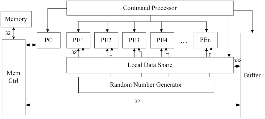
This is a simple GPU with four 32-bit cores . It contains 4 Processing
Elements (PE or core). Each PE has 32 registers, one ALU and Local data
store (LDS). It also includes a random number generator 32 bits 4x8.
It has 16Kx32 bits of memory. The memory is interface with processor with
BUF (buffer unit) connected to LDS. LDS communicates to all PEs in
parallel. NPU operates in Single Instruction Multiple Data (SIMD) mode.
That is, every PE runs the same program in synchrony. So, NPU has only
one control unit. It has one program counter (PC) and one Instruction
Register (IR). Its instruction has fixed size of 32 bits.
Instruction format
op:8 a1:14 a2:5 a3:5
a1 is ads or #n 14 bits
a1 is ls, r3
a2 is r1
a3 is r2
ls 0,1,2,3
r 0..31
Data
ld ls @ads LDS[ls] = M[ads] ls = 0,1,2,3
st ls @ads M[ads] = LDS[ls]
ldr r R[r] = LDS r = 0..31
str r LDS = R[r]
ldx ls r1 r2 LDS[ls] = M[R[r1]+R[r2]] load indirect (index)
stx ls r1 r2 M[R[r1]+R[r2]] = LDS[ls] store index
ldw @ads LDS = M[ads] load wide
bc r ls R[r] = LDS[ls] broadcast
ALU operations
add r3 r1 r2 R[r3] = R[r1] + R[r2]
sub r3 r1 r2 R[r3] = R[r1] - R[r2]
mul r3 r1 r2 R[r3] = R[r1] * R[r2]
ashr r3 r1 #n R[r3] = R[r1] >> n
addi r3 r1 #n R[r3] = R[r1] + n
and r3 r1 r2 R[r3] = R[r1] & R[r2]
or r3 r1 r2 R[r3] = R[r1] | R[r2]
xor r3 r1 r2 R[r3] = R[r1] ^ R[r2]
lt r3 r1 r2 R[r3] = R[r1] < R[r2]
le r3 r1 r2 R[r3] = R[r1] <= R[r2]
eq r3 r1 r2 R[r3] = R[r1] == R[r2]
Control
jmp @ads pc = ads
jz r @ads if R[r] == 0, pc = ads
jnz r @ads if R[r] != 0, pc = ads
Special
rnd r R[r] = random
mvt r3 r1 r2 if R[r3] != 0, R[r1] = R[r2] move if true pseudo
sys 4 stop simulation
equivalent
inc r addi r r #1
dec r addi r r #-1
clr r xor r r r
mov r3 r1 addi r3 r1 #0
LDS can be named "bus interface" (to join a narrow 32-bit bus, with a wide
32x4 -bit bus to cores) or "broadcast unit" because it can do broadcast one
LDS to all cores.
bc r ls LDS[ls] -> all R[r] broadcast
ldw @ads M[ads] -> all LDS load wide
Assembly language
The source file composed of two sections: code and data. The structure of a
source file is as follow:
<code>
.end
<data>
.end
Code section
A line of instruction consists of opcode and its arguments, or a label. A
label begins with ':'. An argument is a number or an address (prefix '@').
An address can refer to a label.
op arg*
:label
arg is
num, @num, @label
A comment starts with ';' and lasts until the end of line. A comment will
be ignored by the assembler.
; comment until end of line
Data section
The data section consists of set-address and data (number). The set-address
command begins with '@' follow by the address.
@ads
num*
Sample program
Mutiply two vectors, each vector has 4 components. We strip components
across cores.
A = B * C
Let A is at @100..103, B at @104..107, C at @108..111, use R[2] for A, R[0]
for B, R[1] for C.
ld 0 @104
ld 1 @105
ld 2 @106
ld 3 @107 ; load B from Mem to LDS
ldr 0 ; move LDS to R[0]
ld 0 @108
ld 1 @109
ld 2 @110
ld 3 @111 ; load C from Mem to LDS
ldr 1 ; move LDS to R[1]
mul 2 0 1 ; R[2] = R[0] * R[1] all cores
str 2 ; move R[2] to LDS
st 0 @100
st 1 @101
st 2 @102
st 3 @103 ; store LDS to Mem
sys 4 ; stop simulation
.end
; data ; initialise Mem
@100
0 0 0 0 ; A
1 2 3 4 ; B
2 3 4 5 ; C
.end
NPU instruction can perform loop iteration using jump, jump-if-zero,
jump-if-not-zero (jmp, jz, jnz). Because NPU is SIMD the condition
zero/not-zero must be true for all PEs (they work in lock-step). For
example, if we want to loop n times: use R[2]
clr 2
addi 2 2 #n
:loop
; perform some action
dec 2
jnz 2 @loop
Accessing an array
ldx and stx are instructions for accessing an array. They use LDS to
indirectly address memory. The access to memory must be "serialised", that
is, each core takes turn to access memory.
ldx ls r1 r2 LDS[ls] = M[ R[r1]+R[r2] ]
R[r1] + R[r2] of core ls is used as an address to read memory into LDS[ls].
stx ls r1 r2 M[ R[r1] + R[r2] ] = LDS[ls]
Similarly, stx uses R[r1]+R[r2] of core ls to address memory and store
LDS[ls] to that address.
Example program to sum elements in an array. The array is terminated with
0.
i = 0
s = 0
while ax[i] != 0
s = s + ax[i]
i++
We show a program that uses all cores to do the same task. (Quite a waste,
but the program is easy to understand)
; r1 s, r2 i, r3 ax[i], r5 &ax
clr 2 ; i = 0
clr 1 ; s = 0
clr 5
addi 5 5 #100 ; base &ax
:loop
ldx 0 5 2 ; get ax[i] to all cores
ldx 1 5 2
ldx 2 5 2
ldx 3 5 2
ldr 3 ; to r3
jz 3 @exit ; ax[i] == 0 ?
add 1 1 3 ; s += ax[i]
inc 2 ; i++
jmp @loop
:exit
sys 4
.end
@100 ; ax[.]
1 2 3 4 5 0
.end
How to use Assembler and
Simulator
The assembler for NPU is "npasm".
c:> npasm < mul.txt > mul.obj
generate "mul.obj", an object code file. To run this object:
c:> npu < mul.obj
The screen will shows internal registers after executing each instruction,
like this:
0: ld 104 0 0
R[0] 0 0 0 0
R[1] 0 0 0 0
R[2] 0 0 0 0
R[3] 0 0 0 0
LDS 1 0 0 0
1: ld 105 1 0
R[0] 0 0 0 0
R[1] 0 0 0 0
R[2] 0 0 0 0
R[3] 0 0 0 0
LDS 1 2 0 0
. . .
4: ldr 0 0 0
R[0] 1 2 3 4
R[1] 0 0 0 0
R[2] 0 0 0 0
R[3] 0 0 0 0
LDS 1 2 3 4
...
10: mul 2 0 1
R[0] 1 2 3 4
R[1] 2 3 4 5
R[2] 2 6 12 20
R[3] 0 0 0 0
LDS 2 3 4 5
. . .
17: sys 4 0 0
R[0] 1 2 3 4
R[1] 2 3 4 5
R[2] 2 6 12 20
R[3] 0 0 0 0
LDS 2 6 12 20
execute 18 instructions 149 cycles
The simulator has defined 2000 words of memory. The limit of a run is 1000
instructions. (You can change by recompile the simulator).
Tools
The package includes : assembler, simulator, sample programs (Windows) npsim4.zip
Only the executable files for MacOS xnpu4.zip
References
Thammasan,
N. and Chongstitvatana, P., "Design of a GPU-styled Softcore on Field
Programmable Gate Array," Int. Joint Conf. on Computer Science and
Software Engineering (JCSSE), 30 May - 1 June 2012, pp.142-146. ( pdf )
Chongstitvatana,
P., "Putting General Purpose into a GPU-style Softcore," Int. Conf. on
Embedded Systems and Intelligent Technology, Jan 13-15, 2013, Thailand. (preprint )
last update 19 Apr 2022