SX chip
It is a stack-based processor. Its ISA is s-code, som v.2 is its
virtual machine. The data path is 32 bits with the design from a
previous 16-bit stack-based processor (ref tencon), the stack machine
with 2 phases control. It uses microprogram in the control unit,
for the purpose of teaching cycle-accurate execution.
S-code
1..9
Add Sub Mul Div Band Bor Bxor Not Eq
10..19 Ne Lt Le Ge Gt Shl
Shr Mod Ldx Stx
20..29 Ret Retv Array End
Get Put Ld St Jmp Jt
30..38 Jf Lit Call -- Inc
Dec Sys Case Fun
format arg:24 op:8
Bop Add..Mod
Uop Not Array
Meaning of instructions
notation
{... top of stack}
M[] memory
SS[] stack segment
value on stack
Ldx {ads
idx} push M[ads+idx]
Stx {ads idx
val} M[ads+idx] = val
Get.a
push SS[fp-a]
Put.a
{val} SS[fp-a] =
val
Ld.a
push M[a]
St.a
{val} M[a] = val
Jmp.d
pc += d
Jt.d
{val} if val != 0
pc += d
Jf.d
{val} if val == 0
pc += d
Lit.a
push a
Inc.a
SS[fp-a]++
Dec.a
SS[fp-a]--
Call.a
pc2 = pc + 1
pc = a
fetch k at pc
; fun.k
SS[fp+k] = fp
; save old fp
fp = fp +
k ; new frame
sp = fp + 1
SS[sp] =
pc2 ; save return ads
pc++
Ret.m
sp = fp -
m ; restore sp
pc = SS[fp+1]
; restore ret ads
fp =
SS[fp] ; restore fp
Retv.m
tmp =
SS[sp] ; return value
sp = fp - m + 1 ; push tmp
SS[sp] = tmp
pc = SS[fp+1]
fp = SS[fp]
auto detect ret/retv
if sp == fp + 1 ; ret
ret.m
else
retv.m
picture of AR
hi mem
..
PC' <- SP
FP' <- FP
..
lv
..
pv <- SP'
..
sp <- SP''
.. <- FP'
lo mem
Data path
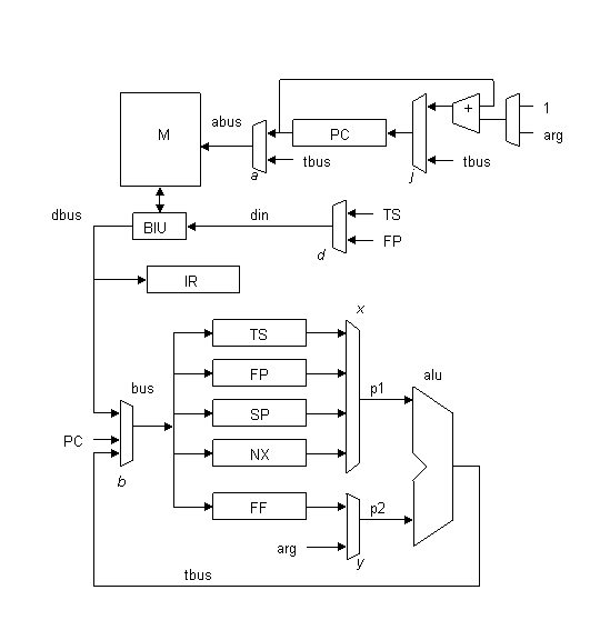
SX caches the top of stack. It has five special purpose registers (no
visible user register): TS, FP, SP, NX, FF, PC is special.
TS top of stack
FP frame pointer
SP stack pointer
NX temp register (next)
FF temp register
To reduce the length of microprogram, will do more in one word.
Using 2 phases enables read-modify-write in one cycle. Reading
from registers and memory will be on positive edge (phi1) and writing
to registers will be on negative edge (phi2). For memory read,
the address is set at phi1, the data is ready at phi2. For memory
write, the address and data are set at phi1, the write signal is
applied at phi2.
The basic cycle is:
read-modify-write
a register
phi1 R -> alu -> tbus
phi2 tbus -> R
mread
phi1
ads -> abus, Mread -> dbus
phi2 dbus -> R
mwrite
phi1
ads -> abus, data -> dbus
phi2 dbus -> Mwrite
reg transfer
phi1
R1 -> tbus
phi2 tbus -> R2
Step-by-step
execution of each instruction
RTL (register transfer language)
stack notation {.. top of stack}
<fetch>
ir = M[pc]
<push x>
sp = sp + 1
M[sp] = x
<pop x>
x = M[sp]
sp = sp - 1
<bop>
pop ff
ts = ts op ff
<uop>
ts = op ts
<get>
push ts
ts = M[fp-arg]
<put>
M[fp-arg] = ts
pop ts
<ld>
push ts
ts = M[arg]
<st> {data}
M[arg] = ts
pop ts
<ldx> {base idx}
pop ff
; base
ts = M[ff+ts]
<stx> {base idx data}
pop nx
; idx
pop ff
; base
M[ff+nx] = ts
pop ts
<jmp>
pc = pc + d
<jt>
if ts != 0
pc = pc + arg
else
pc = pc + 1
pop ts
<jf>
if ts == 0
pc = pc + arg
else
pc = pc + 1
pop ts
<call ads>
return ads is on frame and ts
push ts
; flush stack
ts = pc + 1 ;
ret ads
nx = arg
; save call ads
ir = M[arg] ;
fetch at ads
M[fp+arg] = fp
; save old fp
fp = sp = fp + arg ; new fp, sp
push ts
; save ret ads
pc = nx + 1 ;
jump to body
<ret>
determine ret/retv
return ads is in frame
pc = M[fp+1] ;
restore ret ads
if sp == fp ;
then do ret
sp = fp - arg ; restore sp
pop ts
fp = M[fp]
; restore fp
else
; do retv
sp = fp - arg
fp = M[fp]
pc is special
pc = pc+1, pc+arg, tbus, dbus
mem read cycle
abus (ads to mem) is valid the first
half of cycle
mem read (CE) active the first half of cycle
data is valid before mid cycle
register load pos edge at mid cycle
mem write cycle
abus is valid the first half
data is valid the first half
mem write active the first half and latches data at mid
References
Burutarchanai, A., Nanthanavoot, P., Aporntewan, C., and
Chongstitvatana, P., "A stack-based processor for resource efficient
embedded systems", Proc. of IEEE TENCON 2004, 21-24 November 2004,
Thailand.
Burutarchanai, A., and Chongstitvatana, P., "Design of a two-phased
clocked control unit for performance enhancement of a stack processor",
National Computer Science and Engineering Conference, Thailand, 21-22
Sept. 2004, pp.114-119.
End