Chapter 4
Control unit
A processor is composed of datapath and control unit. Datapath of a processor is the execution unit such as ALU, shifter, registers and their interconnects. Control unit is considered to be the most complex part of a processor. Its function is to control various units in the datapath. Control unit realises the behaviour of a processor as specified by its micro-operations. The performance of control unit is crucial as it determines the clock cycle of the processor.
Control unit can be implemented
by hardwired or by microprogram. A
computer designer strives to optimise three aspects of control unit design:
1.
the complexity (hence cost) of the control unit
2. the speed of control unit
3. the engineering cost of the design (time, correctness etc.)
Hardwired control unit
In the past, hardwired control unit is very difficult to design hence its engineering cost is very high. Presently, the emphasis of computer design is the performance therefore hardwired design is the choice. Also the CAD tools for logic design have improved to the point that a complex design can be mostly automated. Therefore almost all processors of today use hardwired control unit.
Starting with a behavioural description of the control unit, the state diagram of micro-operations is constructed. Most states are simply driven by clock and only transition to the next state. Some states branch to different states depend on conditions such as testing conditional codes or decoding the instruction.
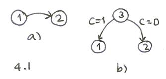
a) event :
go to next state
b) event : go to state 1 or state 2 depends on conditionals
Figure 4.1 several types of states in a state diagram
From the state diagram, a
hardware realization can be constructed almost automatically by some CAD tools.
The in-depth topic of logic design for sequential circuits and logic
minimization can be consulted from many basic textbooks on the subject such as
Katz [KAT93]. The control circuit is implemented using Programmable Logic
Array (PLA). In general, any sequential circuit (which can implement any
state machine) can be constructed from combinational circuits with
feedback. The feedback information is the states. If the feedback
path uses no clock, the circuit is called asynchronous. If the feedback
path uses a latch with clock, the circuit is called synchronous. Synchronous circuits are used almost
exclusively for sequential circuits today as they are easier to design and can
be implemented reliably. Most of the CAD tools handle synchronous
circuits.
Asynchronous circuit has been used for the reason of speed as in many early computer designs, for example, ILLIAC and many computers in the class called supercomputer. But it is difficult to implement reliably and it is still much more difficult to do systematic design of a complex machine using asynchronous circuits. The combinational part of the control circuit can be regarded as a memory where its content is the map of the inputs to the outputs (states are considered to be a part of the outputs). This view of combination circuit as a memory is called Random Access Memory model (RAM) of computation machines.
The bound of complexity of control is States ´ Control inputs ´ Control outputs
Microprogrammed control unit
Maurice Wilkes invented
"microprogram" in 1953 [WIL85]. He realised an idea that made a
control unit easier to design and is more flexible. His idea is that a control
unit can be implemented as a memory which contains patterns of the control bits
and part of the flow control for sequencing those patterns. Microprogram
control unit is actually like a miniature computer which can be
"programmed" to sequence the patterns of control bits. Its
"program" is called "microprogram" to distinguish it from
an ordinary computer program. Using microprogram, a control unit can be
implemented for a complex instruction set which is impossible to do by
hardwired.
Microprogram approach for control
unit has several advantages:
1.
One computer model can be microprogrammed to
"emulate" other model.
2. One instruction set can be used throughout different models of hardware.
3. One hardware can realised many instruction sets. Therefore it is possible to choose the set that is most suitable for an application.
To realise this idea it required
a high speed memory which was not possible at that time. The reason for
speed is that as the control unit determines how fast a sequence of operations
can be executed, the bottle neck becomes the speed of accessing the
microprogram which is stored in a special memory. At IBM, a chief architect of IBM
360 family, Gene Amdahl, has recognised the importance of microprogram and
committed to implement it for IBM 360.
The in-house development for the high speed memory was pursued.
IBM had a great success for her 360 family.
How microprogram work
Like the RAM model, a microprogrammed control unit consists of microPC, micromemory, output buffer and a sequencing unit (Fig 4.2). A micromemory (sometimes called microstore) contains bit patterns that are used to control the datapath. Each word of the micromemory is called "microword". Each word of the micromemory is separated into several fields used for internal control, external control, conditional and specifies the next address. Internal control bits are the signals that control the datapath. External control bits are the signals that control external units such as memory (read, write), interrupt acknowledge etc. Conditionals are the bits that are used to determine the flow of microprogram; loop, branching, next instruction etc. Its input comes from the datapath (usually from the conditional code register). Next address determines the next microword to be executed.
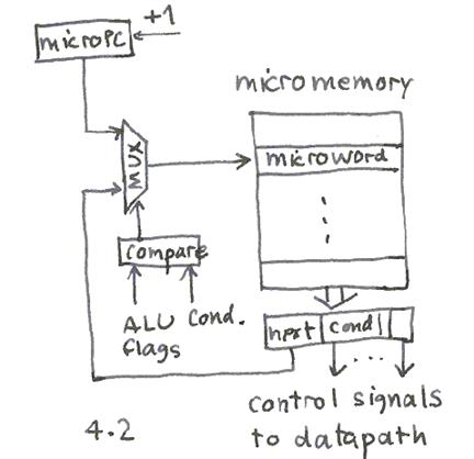
Figure 4.2 a microprogrammed control unit
A microprogram is executed as follow :
1. a word from microprogram at the location specified by the microPC is read out, control bits are latched at the output buffer which is connected to the datapath.
2. if conditional field is specified and the test for conditional is true, the next address of microprogram will come from the next address field otherwise the microPC will be incremented (execute the next microword).
What that has been described is called horizontal microprogram in which there is a one-to-one relationship between internal/external control bits and the actual control signal of the datapath (hence it is wide or "horizontal"). The microword can have other formats. There are several possibilities :
1. single format - one address, as just described above.
2. single format - two addresses, each microword contains two next addresses field, one for result of test true, the other for result of test false.
3. multiple format, such as, one format for the control bits without the next address field and another format for "jump on condition" with the address field. The advantage is that the microword can be shorter than the single format. The disadvantage is that to "jump" will take one extra clock.
Horizontal microprogram allows
each control bit to be independent from other therefore enables maximum
simultaneous events and also offers great flexibility. It is also waste a lot
bit.
For each field of microword, there may be a group of bits that are not activated at the same time therefore they can be "encoded" to use a fewer bit. A decoder is required to "decode" these bits and to connect them to the datapath. This approach is called vertical microprogram. There are many possibilities to compact the micromemory to be as small as possible, sometime trading off speed for space, for example, two-level microprogram. The first level is "vertical" i.e. maximally encoded, the microword of the level one is pointed to the "horizontal word" of the second level. This is rather like the first level is composed entirely from "subroutine call" and the second level is the subroutine.
|
control bits |
next address |
a) one-address format
|
control bits |
true next |
false next |
b) two-address format
|
0 |
control bits |
|
1 |
next address |
c) multiple format
Figure 4.3 several formats of microword
Microprogram becomes obsolete
mainly because the present design emphasizes the performance and microprogram
is slower than hardwired. The change in instruction set design toward a
minimum number of clock per instruction simplifies the instruction set to the
point that microprogram is not really required. Also the design of hardwired
control unit can be mostly automated as opposed to microprogram which must be
written and debug. Hence, for the current instruction set architecture,
hardwired control unit offers a lower engineering cost.
Realisation of microprogrammed systems
This section discusses the
equivalence of hardware and software in realising a sequential system. This concept will be illustrated by a
simple example of designing a 4-bit comparator in both hardwired and
microprogrammed systems (this example is due to [MAN92]).
An assembly of logic elements, whether combinational (AND, OR, NOT, NAND gates, demultiplexors, multiplexor etc) or sequential (flip-flops, registers etc.) is called a "hardwired logic". By incorporating memories and the content of memory is the test or assignment elements, the system is called a "microprogrammed logic system", the content is the "microprogram". A microprogrammed system can be used to realise a synchronous sequential system, that is it can be used to implement a control unit.
Example a 4-bit comparator input : A0 A1 B0 B1 Z is { EQ, LT, GT }. One can write the logic expression of Z as
Z = (A1' B1' A0 B0' + A1 B1' + A1 B1 A0 B0' ) . GT + (A1' B1' A0' B0' + A1 'B1' A0 B0 + A1 B1 A0' B0' + A1 B1 A0 B0 ) . EQ + (A1' B1' A0' B0' + A1' B1 + A1 B1 A0' B0 ) . LT
where A' is NOT A
The expression can be tabulated in the table below :
|
number |
A1 |
B1 |
A0 |
B0 |
Z |
|
0 |
0 |
0 |
0 |
0 |
EQ |
|
1 |
0 |
0 |
0 |
1 |
LT |
|
2 |
0 |
0 |
1 |
0 |
GT |
|
3 |
0 |
0 |
1 |
1 |
EQ |
|
4..7 |
0 |
1 |
X |
X |
LT |
|
8..11 |
1 |
0 |
X |
X |
GT |
|
12 |
1 |
1 |
0 |
0 |
EQ |
|
13 |
1 |
1 |
0 |
1 |
LT |
|
14 |
1 |
1 |
1 |
0 |
GT |
|
15 |
1 |
1 |
1 |
1 |
EQ |
This expression can be represented as a diagram of test and assignment primitives that is traversed sequentially by using synchronous sequential system which each clock reads an element of the diagram and executes the primitive.
Z = compare(A,B)
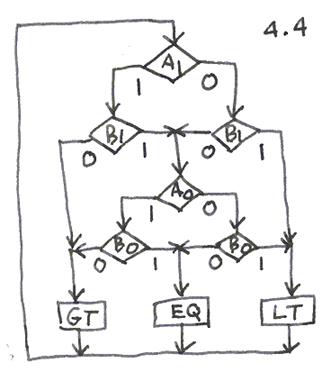
Figure 4.4 diagram of compare
Each primitive can be described as follows:
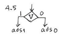
Figure 4.5 test
element
test
if V is true then goto ads1 else goto ads0
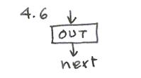
Figure 4.6 assignment element
assignment
output OUT and goto next
The above diagram can be translated into "microprogram" as follows :
0 if A1 then 1 else 2
1 if B1 then 3 else 6
2 if B1 then 8 else 3
4 if A0 then 4 else 5
5 if B0 then 7 else 6
6 R = GT goto 0
7 R = EQ goto 0
8 R = LT goto 0
Next, the microprogram encoded to
map the primitives to a concrete representation. The 4 cases of test inputs {A1 B1 A0 B0}
are encoded into 2 bits. The output
{ EQ LT GT} is encoded into 3 bits using unary code.
|
input |
i1 |
i0 |
|
A1 |
0 |
0 |
|
B1 |
0 |
1 |
|
A0 |
1 |
0 |
|
B0 |
1 |
1 |
|
output |
z2 |
z1 |
z0 |
|
GT |
1 |
0 |
0 |
|
EQ |
0 |
1 |
0 |
|
LT |
0 |
0 |
1 |
The microword has two types: test, assignment. The address field has 4 bits to cover the whole microprogram address (0 . . 8)
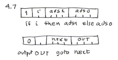
Figure 4.7 microword
format for compare
The microprogram then can be written as follows :
|
ads |
T |
i1
i0 |
ads1, next |
ads0, z |
|
0000 |
1 |
0
0 |
0001 |
0010 |
|
0001 |
1 |
0
1 |
0011 |
0110 |
|
0010 |
1 |
0
1 |
1000 |
0011 |
|
0011 |
1 |
1
0 |
0100 |
0101 |
|
0100 |
1 |
1
1 |
0111 |
0110 |
|
0101 |
1 |
1
1 |
1000 |
0111 |
|
0110 |
0 |
-
- |
0000 |
-100 |
|
0111 |
0 |
-
- |
0000 |
-010 |
|
1000 |
0 |
-
- |
0000 |
-001 |
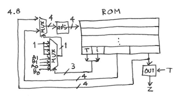
Figure 4.8 microprogrammed unit to realise the
function compare
The microprogrammed unit to
realise the function compare is shown in Fig. 4.8. How many clocks it takes to evaluate
compare (A, B)? Observing the
diagram (Fig. 4.4), on the longest path, there are 5 "steps" to
traverse the diagram hence it takes 5 clocks to evaluate this function using
the microprogrammed unit above.
Equivalence of hardware and software
The definition of microprogramming is due to Wilkes, who in 1953 suggested a method for designing the control unit of a processor, based on the use of sequence of microwords - a microprogram - held in a read only memory (ROM). In this context, microprogramming is generally understood as the technique of producing interpreters for high-level language.
At that time random access memory (RAM) that was available was much slower than the processor, leads to CISC (Complex Instruction Set Computer) to achieve high speed the microprogram of CISC are organised horizontally; the need to control a complex processing unit requires each microword to consist of a large number of bits, often over 100.
Firmware, specification of a
microprogram, is not an interpretation algorithm but a logic system. The concept of vertically organised
microprogram follows that each microword is of fewer bits than in horizontally
organised microprogram. The
resulting simplicity enables a true optimization of the software to be
achieved. Firmware is the
transformation and equivalence between hardware (logic systems) and software
(microprogram). This hardware-software equivalence is a particular case of the
equivalence between space and time
Conclusion
As the history tells us, the
microprocessor followed the same trend as earlier computer designs.
Because of the limit of resource (the number of transistor in a chip),
hardwired control was implemented and the instruction set architecture was
toward a simple design. The advantage of simpler design for control unit
and ease of change popularised microprogramming. Microprogram made it
possible to achieve more complex instruction sets. With a much larger
micro memory a machine as elaborate as the VAX [LEV89] is possible. In
1984, DEC wanted to offer a cheaper machine with the same instruction set as
VAX. They reduced the instructions interpreted by microprogram by
trapping some instructions and performing them in software. They
discovered that 20% of VAX instructions occupied 60% of the microprogram, and
yet they are used (executed) only 0.2% of the time. The simpler subset of
VAX ISA, called MicroVAX-1, implemented 80% of VAX instruction in microprogram,
other 20% is trapped to software, has the size of micro-memory reduced from
480K (VAX) to 64K (MicroVAX-1), and perform 90% of the performance of
VAX-11/780. This is also an evidence toward a new thinking in instruction
set design. The current design sees
the revive of the idea of translating between the real executable code into the
internal code which is suitable for controlling the functional units [GEP00]
[KLA00]. The idea of "code
translation" is used to retain the ISA compatibility for the existing
software to be run on the new hardware.
References
[GEP00] Geppert, L. and Perry, T., Transmeta's magic show, IEEE Spectrum, vol 37, no. 5, May 2000, pp.26-33.
[KAT93] Katz, R., Contemporary Logic Design, Addison-Wesley Pub Co.,
1993.
[KLA00] Klaiber, A., The technology behing Crusoe processors, White
paper, Transmeta Corp., January 2000, http:// www.transmeta.com/ crusoe/
download/ pdf/ crusoetechwp.pdf.
[LEV89] Levy, H. and Eckhouse, R., Computer programming and architecture: The VAX, 2nd ed., Digital press, 1989.
[MAN92] Mange, D., Microprogrammed systems: an introduction to firmware theory, Chapman & Hall, 1992.
[WIL85] Wilkes, M., Memoirs of a computer pioneer, MIT Press, 1985.