Cache memory is a "small" fast memory that resides "between" main memory and the processor. It is much faster than the main memory. Having cache memory reduces the access time. Because cache memory is much smaller than main memory, it is a "copy" of some part of the main memory. When the processor gets the data from cache memory it is called, cache is "hit", otherwise that data has to be fetched from the main memory, in this case, it is called a "miss".
The goal is to arrange the cache memory to maximize "hit".
The main memory can be considered to be divided into many
blocks of cache (in which the actual cache can keep only a few of these
blocks). The full address bit is divided into two parts, the address
bit to cache block, and the address bit to the tag. TAG stores the
"block number" of the actual block of memory stored in the cache at that
moment. In other words, TAG is used to remember which block is
stored in the cache memory.
Organisation
Direct Map
Fully Associative
Set Associative
The simplest organisation of cache is to use the block number to "directly" address the TAG. When an access occurs, the "actual" TAG address bit is compared to the "block number" stored in that slot, if they are the same, it is a hit, otherwise it is a miss.
Let us illustrate by an example:
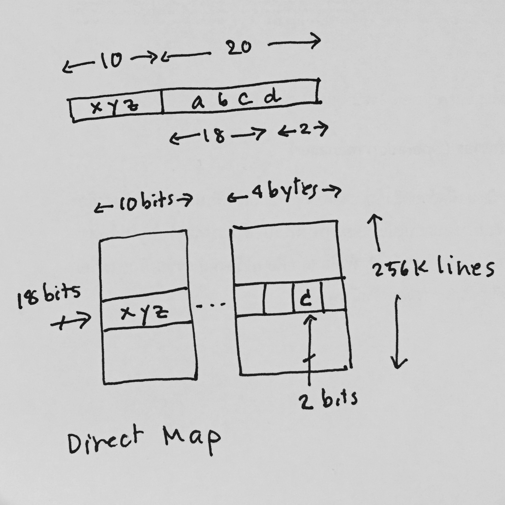
The main memory is 1G bytes (address 30 bits). The
cache is 1M bytes (address 20 bits). The cache is organised as 4 bytes
each line (4 x 256KB). For a direct map cache, we need a TAG storage
which has 256K slots, each slot stores 10 bits of the "block number".
Let the access address be "xyzabcd" where xyz is the left
most 10 bits and abcd is the rest 20 bits. "abcd" is used as
the address of the 1M cache. The leftmost 18 bits points to a line in the
cache and the rightmost 2 bits points to a byte in the line.
"xyz" (10 bits) is the block number stored in the corresponding slot in
the TAG. When an access occurs, the bottom 20 bits of address goes
to cache block with the leftmost 18 bits points to a line (select one of
256K lines). The first 10 bits is compared with the block number in the
corresponding slot in TAG. If they are the same, the access is a hit
and the processor can retrieved the valid data from the cache
memory. If it is a miss, the data will be fetched from the main
memory and also write to cache. The "block number" in the TAG will
be updated.
Direct map organisation is economic to implement.
However, it is restrictive because the access can be conflicting at the
same "block" eventhough there are other slot available.
To improve this situation, the access to TAG storage is change to
"associative".
The cache can be used more effectively if the "block
number" can be placed at any slot of TAG instead of being
forced to a certain place as in the direct map. To do this the TAG
storage must be "associative". This means that the action to access
the "block number" is a kin to answer the question "where xyz exists in
the TAG?" That is the same as using the "content" to address the
memory.
With "associative" TAG storage, the part "xyz" can be placed at any
empty slot. Therefore the hit rate is better than the direct map
organisation. The disadvantage is that "associative" memory is
expensive to implement. The third alternative cache organisation is
the hybrid of direct map and fully associative.
Rather than having full freedom of associative memory,
a number of direct map can be used in parallel (so called a set, or
n-way). All TAG are compared in parallel and there are flexibility
in choosing one of n places to store data.
This scheme keeps simplicity of direct map and it is flexible in
using the available slot (up to n choices).
write through
write back
When all write to cache is also write to the main
memory, the consistency between cache memory and main memory will be
simple to keep. This can be important in some application.
However, always having to write to the main memory will slow down the
access.
In the write back scheme, the main memory will be
update only when there is a miss on that slot. In order to do that,
an extra bit of memory is needed to keep track whether a slot in cache has
been written to or not. This is called the "dirty" bit. When a
write to cache occurs its dirty bit is set. When a miss occurs, the
dirty bit is inspected and if it is set, the content of cache will be
update to the main memory. This method reduces the number of write
to the main memory to the minimum. However, the state of main memory
and the cache memory may not be the same all the time.
As the access pattern of instruction is different from the one of data, it is better to separate cache of instruction and cache of data (to have a better hit for both). However, to maximise the use of of the memory in a cache, "Unified" cache is used. A unified cache stores both instruction and data. One disadvantage of the separate instruction/data cache is that there will be a "fragment" unused in both caches because of the fixed size of both caches. The unified cache can reduce this waste.
Intel twelfth generation processor has large L3 cache. For i5, L3 is 20 MB.
https://www.anandtech.com/show/17162/intel-announces-12th-gen-core-alder-lake-22-new-desktops-cpus-8-new-laptoph-cpus
Intel sixth generation i5 6200U (2016) has 2 cores, 4 threads, with TDP 15W. It has 3 levels of cache: L1 cache 128 K bytes (2 x 32KB 8-way set associative, separate instruction/data), L2 512K bytes (2 x 256KB 4-way) and L3 3072K bytes (12-way).
http://ark.intel.com/products/88193/Intel-Core-i5-6200U-Processor-3M-Cache-up-to-2_80-GHzlast update 28 March 2022